Semiconductor Thin Film Characterization

Thin-film semiconductor technologies are widely employed for transistors and photodiodes in many industrial devices, including active-matrix LCDs, solar panels, camera sensors, solid-state batteries, and flash memory chips. However, the properties of thin films can vary dramatically depending on the conditions during sample preparation, so the optoelectronic properties of these films must be measured and analyzed for different preparation conditions prior to mass production. Specifically, if the refractive index n and the extinction coefficient κ are measured over a wide band, they can be used to determine further optical properties such as the dielectric function.

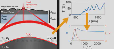
Our lab has developed multiple optimization-based inverse synthesis methods for characterizing the optical properties of thin film semiconductors using spectroscopic measurements taken from transmission spectrophotometers. Our methods are capable of accounting for errors in thin film preparation, such as surface tilts. For instance, we developed an optimization-based characterization method which uses a split-step angular spectrum propagator to model any geometrical properties of a thin film larger than an optical wavelength.

Additionally, our lab has expanded upon the “model-free” methods of characterizing semiconductors, derived from the famous Swanepoel method.

Selected Publications